Showing posts with label diagram. Show all posts
Showing posts with label diagram. Show all posts
Sunday, September 21, 2014
Simple Crystal Tester Circuit Diagram
Simple Crystal Tester Circuit Diagram. Most electronics project working with high frequency utilizes crystal in order to generate frequency as oscillator. It is used instead of coil. Coil can be checked with multi-meter if there is any fault, but checking of crystal completely is difficult. In order to solve this problem a simple project using few components is designed call crystal tester.
This circuit consist two NPN transistors, two diode with few passive component. The crystal under test is combining with transistor T1 which further work as oscillator. The combination of transistor T1, crystal under test and capacitors C1 and C2 is work as colpiitt oscillator. If the testing crystal is good then it works as oscillator with transistor T1. The output of oscillator is rectified and filtered by diode D1 and capacitor C2 respectively and given to base of transistor T2. The signal given to base conduct transistor which further glow the LED connected to the collector through resistor R3. If the testing crystal is faulty then LED1 does not glow.
Simple Crystal Tester Circuit Diagram

PARTS LIST
Resistors (all ¼-watt, ± 5% Carbon unless stated otherwise)
R1 = 27 KΩ
R2 = 1 KΩ
R3 = 560 Ω
Capacitors
C1 = 0.001 µF
C2 = 100 pF
C3 = 0.001 µF
C4 = 0.004 µF
Semiconductors
D1, D2 = 1N4148
T1, T2 = BC550C
LED1 = Green
Miscellaneous
SW1 = push to on switch
Resistors (all ¼-watt, ± 5% Carbon unless stated otherwise)
R1 = 27 KΩ
R2 = 1 KΩ
R3 = 560 Ω
Capacitors
C1 = 0.001 µF
C2 = 100 pF
C3 = 0.001 µF
C4 = 0.004 µF
Semiconductors
D1, D2 = 1N4148
T1, T2 = BC550C
LED1 = Green
Miscellaneous
SW1 = push to on switch
Simple 300w Subwoofer Power Amplifier Wiring Circuit Diagram
Simple 300w Subwoofer Power Amplifier Wiring Circuit Diagram


Subwoofer Speaker Wiring Diagram Subwoofer Review.
Subwoofer Wiring Diagrams Four 4 Ohm Dual Voice Coil Dvc Speakers.
300w Subwoofer Power Amplifier Wiring Diagram
Subwoofer Wiring Diagrams Two 8 Ohm Single Voice Coil Svc Speakers.
Discuss Ep4000 Maelstrom X Ii In The Diy Subwoofers Forum.
Subwoofer Wiring Diagrams Hip Hop Universe.Bazooka Subwoofer Wiring Diagram.
Need Sum Help Wiring Dual Coil Sub And Box Build Trinituner Com.
Car Subwoofer Wiring
Sub 2 Output Is An Excellent Way To Connect Your Subwoofers The Total.
Remote Field Strength Meter Circuit Diagram
Remote Field Strength Meter Circuit Diagram. This field strength meter consists of a tuned crystal detector producing a dc output voltage from a transmitted signal. The dc voltage is used to shift the frequency of a transmitter of 100-mW power operating at 1650 kHz. The frequency shift is proportional to the received field strength. This unit has a range of several hundred feet and is operated under FCC part 15 rules (100-mW max power into a 2-m-iong antenna between 510 and 1705 kHz).
Remote Field Strength Meter Circuit Diagram

Simple Hard Disk Selector Circuit Diagram

In the last few years, the available range of operating systems for PCs has increased dramatically. Various free (!) operating systems have been added to the list, such as BeOS, OpenBSD and Linux. These systems are also available in different colours and flavours (versions and distributions). Windows is also no longer simply Windows, because there are now several different versions (Windows 95, 98, ME, NT, XP, Vista and 7). Computer users thus have a large variety of options with regard to the operating system to be used. One problem is that not all hardware works equally well under the various operating systems, and with regard to software, compatibility is far from being universal. In other words, it’s difficult to make a good choice.
Hard Disk Selector Circuit Diagram

Switching from one operating system to another - that’s a risky business, isn’t it? Although this may be a bit of an exaggeration, the safest approach is still to install two different operating systems on the same PC, so you can always easily use the ‘old’ operating system if the new one fails to meet your needs (or suit your taste). A software solution is often used for such a ‘dual system’. A program called a ‘boot manager’ can be used to allow the user to choose, during the start-up process, which hard disk will be used for starting up the computer. Unfortunately, this does not always work flawlessly, and in most cases this boot manager is replaced by the standard boot loader of the operating system when a new operating system is installed.
In many cases, the only remedy is to reinstall the software. The solution presented here does not suffer from this problem. It is a hardware solution that causes the primary and secondary hard disk drives to ‘swap places’ when the computer is started up, if so desired. From the perspective of the computer (and the software running on the computer), it appears as though these two hard disks have actually changed places. This trick is made possible by a feature of the IDE specification called ‘CableSelect’. Every IDE hard disk can be configured to use either Master/Slave or CableSelect. In the latter case, a signal on the IDE cable tells the hard disk whether it is to act as the master or slave device. For this reason, in every IDE cable one lead is interrupted between the connectors for the two disk drives, or the relevant pin is omitted from the connector.


This causes a low level to be present on the CS pin of one of the drives and a high level to be present on the CS pin of the other one (at the far end of the cable). The circuit shown here is connected to the IDE bus of the motherboard via connector K1. Most of the signals are fed directly from K1 to the other connectors (K2 and K3). An IDE hard disk is connected to K2, and a second one is connected to K3. When the computer is switched on or reset, a pulse will appear on the RESET line of the IDE interface. This pulse clocks flip-flop IC1a, and depending on the state of switch S1, the Q output will go either high or low. The state on the Q output is naturally always the opposite of that on the Q output. If we assume that the switch is closed during start-up, a low level will be present on D input of IC1a, so the Q output will be low following the reset pulse.
This low level on the Q output will cause transistor T1 to conduct. The current flowing through T1 will cause LED D1 to light up and transistor T2 to conduct. The hard disk attached to connector K2 will thus see a low level on its CS pin, which will cause it to act as the master drive and thus appear to the computer as the C: drive. A high level will appear on the Q output following the reset pulse. This will prevent T3 and T4 from conducting, with the consequence that LED D2 will be extinguished and the hard disk attached to connector K3 will see a high level on its CS pin. For this disk, this indicates that it is to act as a slave drive (D: drive).
If S1 is open when the reset pulse occurs, the above situation is of course reversed, and the hard disk attached to connector K2 will act as the D: drive, while the hard disk attached to connector K3 will act as the C: drive. Flip-flop IC1a is included here to prevent the hard disks from swapping roles during use. This could have disastrous consequences for the data on the hard disks, and it would most likely cause the computer to crash. This means that you do not have to worry about affecting the operation of the computer if you change the switch setting while the computer is running. The state of the flip-flop, and thus the configuration of the hard disks, can only be changed during a reset.
The circuit is powered from a power connector for a 3.5-inch drive. This advantage of using this connector is that it easily fits onto a standard 4-way header. However, you must observe the correct polarity when attaching the connector. The red lead must be connected to pin 1. Constructing the hard disk selector is easy if the illustrated printed circuit board is used. You will need three IDE cables to connect the circuit. The best idea is to use short cables with only two connectors, with all pins connected 1:1 (no interruption in the CS line). The IDE connector on the motherboard is connected to K1 using one cable. A cable then runs from K2 to first hard disk, and another cable runs from K3 to the second hard disk. This means that it is not possible to connect more than two hard disks to this circuit. You must also ensure that the jumpers of both disk drives are configured for CableSelect. To find out how to do this, refer to the user manual(s) for the drives.
Build a Precision full wave Rectifier Circuit Diagram
This Precision full wave Rectifier Circuit Diagram provides accurate full wave rectification. The output impedance is low for both input polarities, and the errors are small at all signal levels. Note that the output will not sink heavy current, except a small amount through the 10K resistors. Therefore, the load applied should be referenced to ground or a negative voltage. Reversal of all diode polarities will reverse the polarity of the output
Since the outputs of the amplifiers must slew through two diode drops when the input polarity changes, 741 type devices give 5% distortion at about 300 Hz.
Precision full wave Rectifier Circuit Diagram
Since the outputs of the amplifiers must slew through two diode drops when the input polarity changes, 741 type devices give 5% distortion at about 300 Hz.
Precision full wave Rectifier Circuit Diagram

Sourced By: http://circuitsstream.blogspot.com/2013/07/precision-full-wave-rectifier-circuit.html
TL496 3 to 9 volt converter Circuit Diagram
This is simple Simple TL496 3 to 9 volt converter Circuit Diagram. it uses the TL496 power supply controller, a coil and a electrolytic capacitor. The maximum output voltage is actually 8.6V and current is around 80mA.The input current (the current drawn from the batteries) is 405mA at the maximum output current. Without load the current consumption is 125µA and the batteries life is around 166 days.
TL496 3 to 9 volt converter Circuit Diagram

Simple Telephone In Use Indicator Circuit Diagram
This is a Simple Telephone In Use Indicator Circuit Diagram. With this circuit mounted in or near every phone in the house, it will allow users to know if the phone is being used and not to pick up the phone. When a phone is taken off hook, the voltage across the tip and ring terminals drops to 10 volts or less. This will cause the FET (2N4360) to turn on and also turn on the transistor (2N2222). When the transistor turns on it will allow current to flow through the LED and make it light. A blinking LED could be used to make the effect better.
Simple Telephone In Use Indicator Circuit Diagram

Build a 12V 7 2Ah SMF Battery Charger Circuit Diagram
Build a 12V 7.2Ah SMF Battery Charger Circuit Diagram. The LM317 is an adjustable three-terminal positive-voltage regulator capable of supplying more than 1.5A over an output-voltage range of 1.25 V to 37 V. It is exceptionally easy to use and requires only two external resistors, R2’ and R2” (R2= R2’+ R2”) to set the output voltage. Furthermore, both line and load regulation is better than standard fixed regulators. In addition to having higher performance than fixed regulators, this device includes on-chip current limiting thermal overload protection, and safe-operating-area protection. All overload protection remains fully functional, even if the ADJUST terminal is disconnected. By connecting a fixed resistor, R1 the ADJUST and OUTPUT terminals, the LM317 can function as a precision current regulator. An optional output capacitor can be added to improve transient response.
Schematic Diagram using LM317

The ADJUST terminal can be bypassed to achieve very high ripple-rejection ratios, which are difficult to achieve with standard three-terminal regulators. A capacitor of small value should be connected across the input pin of LM317 and ground, particularly if the regulator is not in close proximity to the power-supply filter capacitor.
Please note that the output can go no lower than 1.25 Volts.The Input voltage must be about 3 Volts above the desired Output Voltage. So input voltage should be around 18V.So a transformer with the secondary voltage of 17 V is used.
Determining the Values
Vo is calculated by following formula , Vo = Vref * ( 1 + R2/R1 )
Where Vo is the voltage drop across the output i.e voltage applied to the charge the battery.
Here Vref = 1.25.Making R1 a standard value, like 220 Ohms sets the current through R2 as well. Now all we have to do is select the value of R2 to give us a voltage drop of our desired V OUT, minus the 1.25 Volts across R1.
So for Vomaximum=15 v and Vominimum=12 v we get respective values of R2minimum=1K8 and R2maximum=2K3 which we will get by keeping R2’=1k8 and R2”=500 Ohms (variable).
The most commonly used OPAMPS are 741 and 324. IC741 is used in close loop configuration and LM324 in open loop configuration. i.e. LM324 mainly used as comparator while 741 for amplification,addition etc
LM317 regulates the Output at 1.25 Volts above the Reference pin. Knowing this the value of this resistor sets the current through both resistors. The current drawn by the Reference pin is small and can be ignored as long as the current through the resistors is around 1 mA to 10 mA.
Testing your Circuit
Output voltage can be varied and obtained as wanted(between 12v and 15v,minimum and maximum charging voltages. Observed voltage values at INPUT ,OUTPUT and ADJUST pins is shown in table.While testing take enough precaution as not to short OUTPUT and ADJUST pins as it may damage the transistor BC 547,whose collector is connected to adjustment pin.
| ADJUST | OUTPUT | INPUT | Vref |
| 13.7 V | 12.47 V | 15.01 V | 1.23 |
The difference between voltage at output pin and adjustment pin is 1.23 (~1.25) which is the reference voltage Vref. Current rating of battery to be charged 7.2 Ah 12v, short circuit current Isc = 720mA .Using multi-meter check the short circuit current.If the Isc shows a different value than expected,it can be changed by increasing or decreasing the load connected between the emitter of the transistor T1 and ground.
Working of Charger Circuit
The circuit uses two LEDs as indicators; one for signaling charging ON condition,and the other as an indicator , when charging voltage falls below its terminal voltage (~12 volts). Terminal voltage can be adjusted by adjusting the 1k Trimpot. The output voltage range can be adjusted by 500 ohm Trimpot. LM324 is used in comparator circuit,after the rectifier circuit. Comparator will compare the voltage levels,and if the output voltage is less than the charging voltage,the voltage across the red LED will go high thus indicating drop in charging voltage.

Diode Protection for LM317T
If the battery is connected to the charger but unplugged from the power source, you end up with the input voltage of the circuit disconnected while the output voltage is still present. Some regulators can be damaged by this, and thus diodes are put into the circuit to protect them.
Applications
SMF batteries or VRLA batteries (valve-regulated lead-acid battery) are made in an eco-friendly, ISO Certified & modern plant with a large manufacturing capacity and are being sold worldwide. There is a wide range available to suit all applications of standby power requirement’s, for example:
- UPS (Uninterrupted power supply)
- Inverter and Emergency Lights
- Telecommunication equipment
- Fire Alarm & Security Systems
- Railway Signaling
- Electronic Attendance & Cash Registers
- Solar Lanterns and Systems,
etc. come in factory charged conditions and have a high shelf life thereby requiring longer time intervals between recharging of batteries in stock. Source : Link
1KHz Sinewave Generator Circuit Diagram
Simple circuitry, low distortion, battery operated Variable, low impedance output up to 1V RMS
Circuit diagram
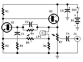
Parts:
- R1 5K6 1/4W Resistor
- R2 1K8 1/4W Resistor
- R3,R4 15K 1/4W Resistors
- R5 500R 1/2W Trimmer Cermet
- R6 330R 1/4W Resistor
- R7 470R Linear Potentiometer
- C1,C2 10nF 63V Polyester Capacitors
- C3 100µF 25V Electrolytic Capacitor
- C4 470nF 63V Polyester Capacitor
- Q1,Q2 BC238 25V 100mA NPN Transistors
- LP1 12V 40mA Lamp (See Notes)
- J1 Phono chassis Socket
- SW1 SPST Slider Switch
- B1 9V PP3
- Clip for 9V PP3 Battery
Circuit description:
This circuit generates a good 1KHz sinewave using the inverted Wien bridge configuration (C1-R3 & C2-R4). Features a variable output, low distortion and low output impedance in order to obtain good overload capability. A small filament lamp ensures a stable long term output amplitude waveform. Useful to test the Audio Millivoltmeter, Audio Power Meter and other audio circuits published in this site.
Notes:
- The lamp must be a low current type (12V 40-50mA or 6V 50mA) in order to obtain good long term stability and low distortion.
- Distortion @ 1V RMS output is 0.15% with a 12V 40mA lamp, raising to 0.5% with a 12V 100mA one.
- Using a lamp differing from specifications may require a change in R6 value to 220 or 150 Ohms to ensure proper circuits oscillation.
- Set R5 to read 1V RMS on an Audio Millivoltmeter connected to the output with R7 fully clockwise, or to view a sinewave of 2.828V Peak-to-Peak on the oscilloscope.
- With C1,C2 = 100nF the frequency generated is 100Hz and with C1,C2 = 1nF frequency is 10KHz but R5 is needing adjustment.
- High gain transistors preferred for better performance.
Build a Power On Reset Circuit Diagram
This is a simple power on switching circuit. This type of reset pulse is ideally provided by this circuit. Because of the high input impedance of the Schmidt trigger, long reset pulse times may be achieved without the excess dissipation that results when both output devices are on simultaneously, as in an ordinary gate device (B). A reset pulse is often required at power-on in a digital system. See circuit diagram below.
Simple Power On Reset Circuit Diagram

Audio Milli Volt Meter Circuit Diagram
Build a simple audio Milli volt meter circuit diagram. This Audio Milli Volt Meter Circuit has a flat response from 8Hz to 50 kHz at -3 db on tbe 10-mV range. The upper limit remains the same on tbe less sensitive ranges, but the lower frequency limit covers under 1 Hz.
Simple Audio Milli Volt Meter Circuit Diagram

Sourced By : http://circuitsdiagram-lab.blogspot.com/2013/11/simple-audio-milli-volt-meter-circuit.html
Crystal Controlled Reflection Oscillator Circuit Diagram
How to build a Crystal-controlled-reflection-oscillator circuit diagram . This is a simple crystal controlled reflection oscillator circuit, this unit is easily tunable and stable, consumes little power, and costs less than other types of oscillators tlmt operate at the same frequencies. This unusual combination of features is made possible by a design concept that includes operation of the transistor well beyond the 3 dB frequency of its current-versus- frequency curve.
Crystal Controlled Reflection Oscillator Circuit Diagram

The concept takes advantage of newly available crystals that resonate at frequencies up to about 1 GHz.The emitter of transistor Q is connected with variable capacitor Cl and series-resonant crystal X. The emitter is also connected to ground through bias resistor Rl. The base is connected to the parallel combination of inductor L and capacitor C3 through DE-blocking capacitor and C4 and is forward biased with respect to the emitter by resistors R3 and R4.
Impedance Z could be the 220-0 resistor shown or any small impedance that enables the extraction of the output signal through coupling capacitor C2. If Z is a tuned circuit, it is tuned to the frequency of the crystal.
Sourced by : http://circuitsdiagram-lab.blogspot.com/2013/11/build-crystal-controlled-reflection.html
Audio Milli Volt Meter Circuit Diagram
This is a simple audio Milli volt meter circuit diagram. This Audio Milli Volt Meter Circuit has a flat response from 8Hz to 50 kHz at -3 db on tbe 10-mV range. The upper limit remains the same on tbe less sensitive ranges, but the lower frequency limit covers under 1 Hz.
Simple Audio Milli Volt Meter Circuit Diagram
Wednesday, June 5, 2013
Basic Thermostat Wiring Diagram
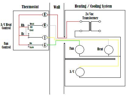
Basic Thermostat Wiring Diagram.

Thermostat Components Thermostat Boiler Troubleshooting.

Digital Thermostat Duotherm Wiring Diagram 1 Jpg.

State Select Hot Water Heater Thermostat Wiring Diagram Gif.
Thermostat Wiring Diagram.

Thermostats Edge Thermostat By Carrier.

Wiring Diagram Of Nuheat Solo Programmable Thermostat Around.

Thermostat Wiring Diagram 1 Jpg.

Blue Wire Is Common This Is Optional Since Most Thermostats Have.

Wiring For New Thermostat Heating Air Conditioning.
Tuesday, June 4, 2013
Ethernet Cable Wiring Diagram Crossover

Ethernet Cable Wiring Diagram Crossover Lg.

Ethernet Stp Outdoor Ethernet Cable 1000ft Cat5e 568b Wiring.

Cat 5 Utp Ethernet Crossover Cable How To Tips And Diy Guideline.

Wiring Cables Cabling Fiber Cat3 Cat5e Cat6 Coaxial Gigabit Ethernet.

Crossover Ethernet Cable.

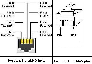
Rj45 Wiring Diagrams.

The Basics Of Network Cable Testing Learn Networking Com.

How To Make A Rj45 Cable Tester.
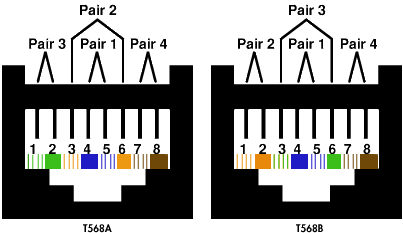
Well Rj45 Receptacle Wiring For Both Standards Are Shown Below.
Ethernet Cables By Karl Shoemaker Ak2o.
Monday, June 3, 2013
Information Honda Cb100 Electrical Wiring Diagram

Headphone Wiring Diagram Headphone Jack Wiring Diagram Iphone Earphone.

More Information About Honda Cb100 Electrical Wiring Diagram Here.

B4000 Anti Lock Brake Circuit And Wiring Diagrams Circuit Schematic.

Wiring Diagram And Cable Harness Schematic The Wiring Diagram.

Blazer Fuse For Heater Fan 1998 Dodge Ram 1500 Radio Wiring Diagram.

Find Detail The 1999 Mitsubishi Carisma Car Wiring Diagram Here.

Air Conditioner 99 Camry Thru Wall Air Conditioner.

Aprilia Rs125 Ignition System Wiring Diagram.

Air Conditioning Wire Diagram Wiring Diagram.

Explain On How To Read A Relay Wiring Diagram Pdf Sb.
Subscribe to:
Posts (Atom)

